Menlo Systems product:

Original publication:
Nanochannels for molecular behavior in confinement
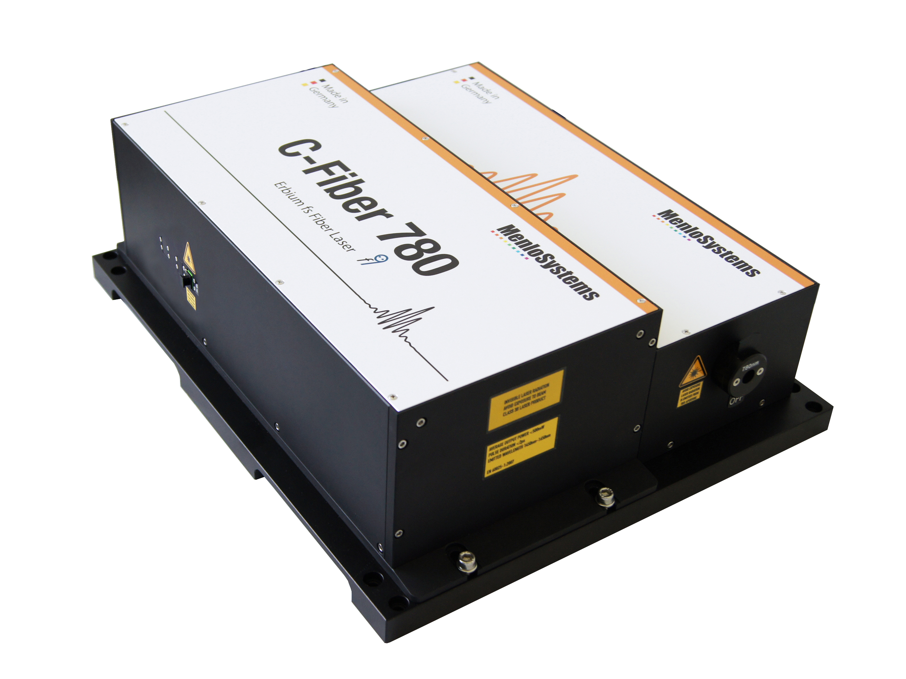
In their recently presented method for scalable fabrication of nanofluidics, researchers from the University of Cambridge used Menlo Systems' C-Fiber 780 femtosecond laser for two-photon nanolithography.
Lab-on-a-chip (LOC) devices - small structures bearing miniature laboratory functions - are generally complex in fabrication but facilitate a wide range of tasks that need to be addressed on small scales. Similar to electronic integrated circuits, which operate with metal-oxide-semiconductor transistors, LOC devices use nanofluidics for the characterization and control of fluid systems in a chip like manner. Due to the extremely reduced channel dimension in the range of sub-100 nanometers, the behavior of the contained fluids significantly differs from their micro- or macroscale counterparts. In particular, the confinement allows observing new physical behavior occurring, within or below the so called Debye length, a measure of the electrostatic potential shielding of charged particles in a solution. Nanofluidics therefore bring new analytical and handling possibilities in biotechnology, medicine, and also in the optimization of reverse electrodialysis power plants for efficient generation of renewable energy. A group of researchers from the University of Cambridge, UK, presents an easy and cost-efficient method for a combined fabrication of nanofluidics and microfluidics which is compatible with existing techniques. They use Menlo Systems' C-Fiber 780 femtosecond laser for two-photon direct laser writing (DLW) of nanochannels into microstructures that have been previously prepared by UV-photolithography.

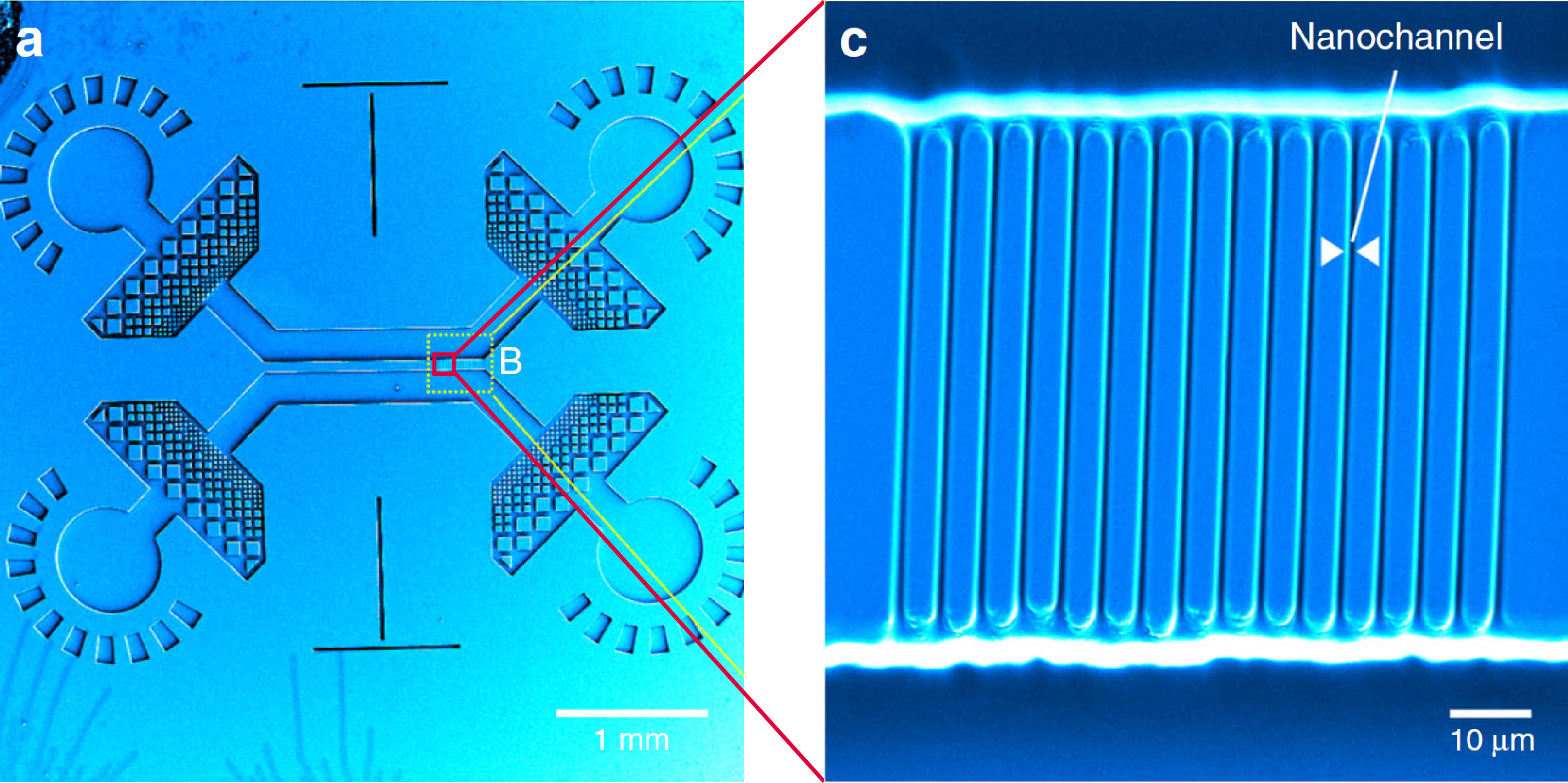
Figure: Details of a nanofluidic device fabricated by combining UV mask lithography and two-photon writing with subsequent soft lithography (Image adopted from original publication)
The analysis of processes in biophysical systems occurring on the molecular scale requires highest precision and the possibility of controlling the environment of the process. Today, scientists are able to observe processes ongoing inside individual cells, and to study single nucleation events governing the folding behavior of proteins. They combine analytical methods available in experimental physics and chemistry with the use of micro- and nanofluidic devices for the confinement of the sample under investigation. Since particles confined within nanometer-sized containers are more influenced by the surrounding electrostatic fields from the channel walls, nanofluidics is a tool to study the impact of the channel size on selective particle transport mechanisms. Therefore, apart from a mere confinement, separation or sorting function for various types of chemical or biological samples, nanochannels are also used to realize membranes that allow exchange of charged particles as needed in reversed electrodialysis (RED) - a technique to retrieve electrical energy from the salinity gradient when mixing seawater and river water, so called “blue energy”.
The fabrication of nanofluidic devices currently involves expensive and time-consuming methods such as electron beam lithography or focused ion beam etching, which both require clean room conditions. This substantially limits the availability of nanofluidics to a narrow range of applications. Moreover, these methods struggle to provide a link between the nanostructures and larger structures for practical applications beyond scientific laboratories. The Cambridge group of researchers describes a novel fast fabrication method which not only presents a viable way to link the production lines of micro- and nanofluidics, but is likewise able to interface nanofluidic devices with the macroscopic world. The interfacing with the environment transfers nanofluidics from the status of fundamental research to real-life applications.
The UK researchers combine conventional UV photolithograpy for microsctructuring and two-photon DLW for nanostructuring of devices into one hybrid production process. The substrate is a photoresist which has been spin coated onto a silicon wafer. In a first step, the microfluidic sections are patterned onto the photoresist by UV exposure through a suitable mask. Secondly, the wafer is baked in order to polymerize the UV-irradiated areas. This induces refractive index changes between areas of UV exposure and masked areas, defining locations of interest for the nanojunctions. In a third step, the nanojunctions are directly written into the photoresist by two-photon lithography, a process which polymerizes the photoresist with nanometer resolution. At last, the unpolymerized photoresist is removed by development in a solvent, leaving the patterned structures on the silicon surface. The cleaned and dried wafer then serves as a master mold for soft lithography. Similar to a stamp, it transfers the micro- and nanofeatures into an elastomeric material.
Compared to UV photolithography, which is ideal for patterning of larger areas, DLW does not need a mask and it is able to produce arbitrary shapes. The resulting features are not dependent on the thickness of the photoresist coating and can be located near or at the substrate surface. However, both UV photolithography and DLW at UV laser wavelength are linear processes, and the achievable feature size is diffraction limited to the micrometer range. In contrast, the method of two-photon DLW applied by the group is a nonlinear process in two aspects: First, two-photon absorption takes place only within a region of high laser intensity, i.e. where the square intensity is above the polymerisation threshold. This volume is smaller than the diffraction limited focal spot of the laser. Second, the nonlinear response of the photoresist similarly further reduces the volume of polymerization. Using Menlo Systems C-Fiber 780 femtosecond fiber laser at 780 nm wavelength the Cambridge group demonstrates two-photon direct laser writing of channels with down to 230 nm lateral width and sub-50 nm height. By means of a calibration assay, the group had previously identified optimal parameters for the laser power, scanning speed, and focal spot offset from the wafer surface, and has finally characterized the obtained structures with scanning electron microscopy (SEM) and atomic force microscopy (AFM).
The novel combined technique is significantly faster than DLW alone, and none of the processing steps requires cleanroom conditions. Moreover, it allows implementing nano-sized functionalities into selected areas of interest, even in existing microfluidic devices. This rapid and cost-efficient method of fabricating nanofluidics is affordable and practicable for biological laboratories and facilitates their fabrication on a larger scale. The Cambridge researchers demonstrated the functionality of their nanodevices by filling them with Rhodamine dye and localizing single molecules with super resolution microscopy imaging methods to resolve the sub-wavelength sized channels.
Author: Patrizia Krok
Original publication:
O. Vanderpoorten et al.: Scalable integration of nano-, and microfluidics with hybrid two-photon lithography; Microsystems & Nanoengineering Vol. 5, No. 40 (2019)